My current research mainly focuses on studying the electronic, optical and mechanical properties of 2D semiconductors. Below I introduce this fascinating family of materials and briefly describe some of my most relevant scientific results.
2D Materials
Two-dimensional (2D) materials are a new family of crystalline materials consisting of a single layer of atoms. The first 2D material to be discovered was Graphene (a single layer of carbon atoms arranged in a hexagonal lattice), firstly isolated by Konstantin Novoselov and Andre Geim in 2004. In the following years, many other 2D crystals have been discovered, each one with different electronic, optical and mechanical properties, and their study has revealed a vast collection of exotic behaviours not observed in three-dimensional materials. 2D materials have found applications in diverse fields such as semiconductor electronics, optoelectronics, or energy storage.
|
Identification of single-layer crystals
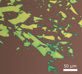
2D crystals are typically obtained by mechanical exfoliation of van der Waals crystals with adhesive or viscoelastic stamps and later transferred onto a SiO2/Si substrate. This results in samples containing a dispersion of crystals of different thicknesses, among which only a small percentage are atomically thin. Thus, identifying monolayer crystals in these samples can be very challenging. Quantitative optical microscopy provides a fast and reliable non-invasive method to determine the thickness of these crystals. In this work we demonstrated how this method can be applied to atomically thin TaSe2 crystals. We also applied this technique in TaS2 crystals [link] and showed how the optical contrast of atomically thin crystals can be improved by using Si3N4/Si substrates, making their identification easier [link]. |
|
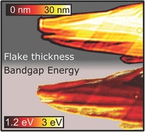
In2Se3 flake thickness vs bandgap energy
|
Hyperspectral imaging
The optical properties of atomically thin materials can show spatial fluctuations due to the presence of strain, thermal gradients, thickness variations, etc. In this work we introduced a hyperspectral imaging technique that allows to probe the optical properties of these materials with diffraction‑limited spatial resolution, and used it to map the spatial variation of exciton resonances in single and few-layer MoS2 crystals. In a different work [link], we also used this technique to characterize the optical absorption spectra of atomically thin α‐In2Se3 crystals. |
|
Strain engineering
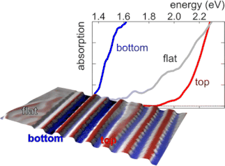
Two-dimensional crystals can withstand very large deformations before rupture. This opens the possibility of modifying the crystal structure and properties by mechanical strain engineering. In this work we studied the effect of strain in the optical response of black phosphorus. By subjecting multilayer black phosphorus sheets to periodic stress we were able to modulate their optical bandgap by up to∼ 0.7 eV between the regions under tensile and compressive stress. In a later work [link] we also studied the effect of local strain in the electronic transport through vertical metal/MoS2/metal structures, using a conductive AFM tip to apply load forces to the MoS2 surface while measuring the I–V characteristics of the contacts. |
|
High-quality 2D phototransistors
Due to their large surface‑to‑volume ratio, the mechanical and electronic properties of 2D materials are extremely sensitive to the surrounding environment. In this work we used atomic force microscopy (AFM) measurements to show how using h-BN substrates can largely reduce the surface roughness of monolayer MoS2 crystals, leading to an improved electrical performance. Another limiting factor for the performance of 2D devices is the quality of electronic contacts. Usually, metallic electrodes are fabricated by metal evaporation directly on top of a 2D semiconductor. However, the performance of the resulting devices is often limited by the formation of Schottky barriers and emergence of fermi level pinning near the electrical contacts. In this other work I explain how these effects can be prevented by inserting a bilayer h-BN layer as tunnel barrier between the electrode and the 2D semiconductor.
Due to their large surface‑to‑volume ratio, the mechanical and electronic properties of 2D materials are extremely sensitive to the surrounding environment. In this work we used atomic force microscopy (AFM) measurements to show how using h-BN substrates can largely reduce the surface roughness of monolayer MoS2 crystals, leading to an improved electrical performance. Another limiting factor for the performance of 2D devices is the quality of electronic contacts. Usually, metallic electrodes are fabricated by metal evaporation directly on top of a 2D semiconductor. However, the performance of the resulting devices is often limited by the formation of Schottky barriers and emergence of fermi level pinning near the electrical contacts. In this other work I explain how these effects can be prevented by inserting a bilayer h-BN layer as tunnel barrier between the electrode and the 2D semiconductor.
|
Exciton physics in 2D materials
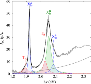
The reduced electron-electron screening in 2D semiconductors often leads to large exciton binding energies and lifetimes. In consequence the optical response of these systems is often dominated by excitonic transitions. In this work I used photocurrent spectroscopy to study the excitonic absorption of a monolayer MoSe2 phototransistor. Very recently we have assembled a new measurement system that allows to perform photocurrent spectroscopy measurements at very low temperature, down to 3 degrees Kelvin [link]. |
|
